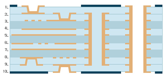
HDI PCB Structure
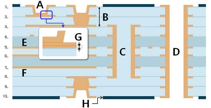
A. LVH (Laser Via Hole)
B. Stacked Via
C. BVH (Buried Via Hole)
D. PTH (Plated Through Hole)
E. CCL (Copper Clad Laminate)
F. P/P (Prepreg)
G. C/F (Copper Foil)
H. S/R Ink (Solder Resist Ink)
Any Layer
 |
 |
| Structure | Cross Section |
|---|
- Specification
| Type | Material | Board Thickness | Min Line Space |
|---|---|---|---|
| All Stack Via | FR-4 | 0.65~1.0T (±10%) | 0.03/0.04 |
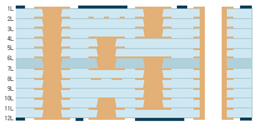
4D Type
 |
 |
| Structure | Cross Section |
|---|
- Specification
| Layer Count | Material | Board Thickness | Min Line Space |
|---|---|---|---|
| 10 Layer | FR-4 | 0.65~1.0T(±10%) | 0.04/0.04 |
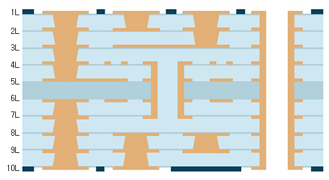
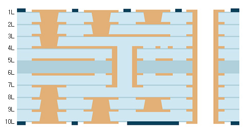
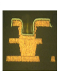
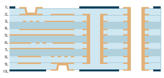
3D Type
 |
 |
| Structure | Cross Section |
|---|
- Specification
| Layer Count | Material | Board Thickness | Min Line Space |
|---|---|---|---|
| 10 Layer | FR-4 | 0.6~1.0T(±10%) | 0.04/0.04, 0.04/0.085 |
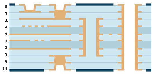
D Type
 |
 |
| Structure | Cross Section |
|---|
- Specification
| Layer Count | Material | Board Thickness | Min Line Space |
|---|---|---|---|
| 10 Layer | FR-4 | 0.8T | 0.04/0.04, 0.05/0.05 |
C Type
 |
 |
| Structure | Cross Section |
|---|
- Specification
| Layer Count | Material | Board Thickness | Min Line Space |
|---|---|---|---|
| 10 Layer | FR-4 | 0.65~0.8T | 0.04/0.04, 0.05/0.05 |
B Type
 |
 |
| Structure | Cross Section |
|---|
- Specification
| Layer Count | Material | Board Thickness | Min Line Space |
|---|---|---|---|
| 10 Layer | FR-4 | 0.65~0.8T | 0.04/0.08, 0.05/0.05 |
BVH Type
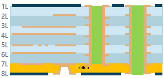 |
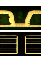 |
| Structure | Cross Section |
|---|
- Specification
| Layer Count | Material | Board Thickness | Min Line Space |
|---|---|---|---|
| 8 Layer | FR-4, Teflon | 0.9~1.1T | 0.12/0.15 |